
In this tutorial, we will explore transistors in detail, discussing their definition, fundamental principles, different types, and uses. Let’s begin!
What is a transistor?
The transistor is a semiconductor device that acts like a switch in electronic circuits. A transistor can be turned OFF and ON as needed like a switch. Transistors are also used in the amplification process. In this blog, we will learn about the basics of BJT(Bipolar junction transistor) transistor.
Construction of transistor
The transistor consists of three layers of semiconductor. They can be PNP or NPN. PNP transistor has two P-type semiconductors and one N-type semiconductor. On the other hand, an NPN transistor has two N-type semiconductors and one P-type semiconductor.
In between two same type semiconductors one different type of semiconductor is injected. This middle part of the transistor is the base. Among the other two semiconductors, one is an emitter and the other one is a collector. The base and collector are lightly doped and the emitter is highly doped. The emitter is indicated by E, the base is indicated by B, and the collector is indicated by C.
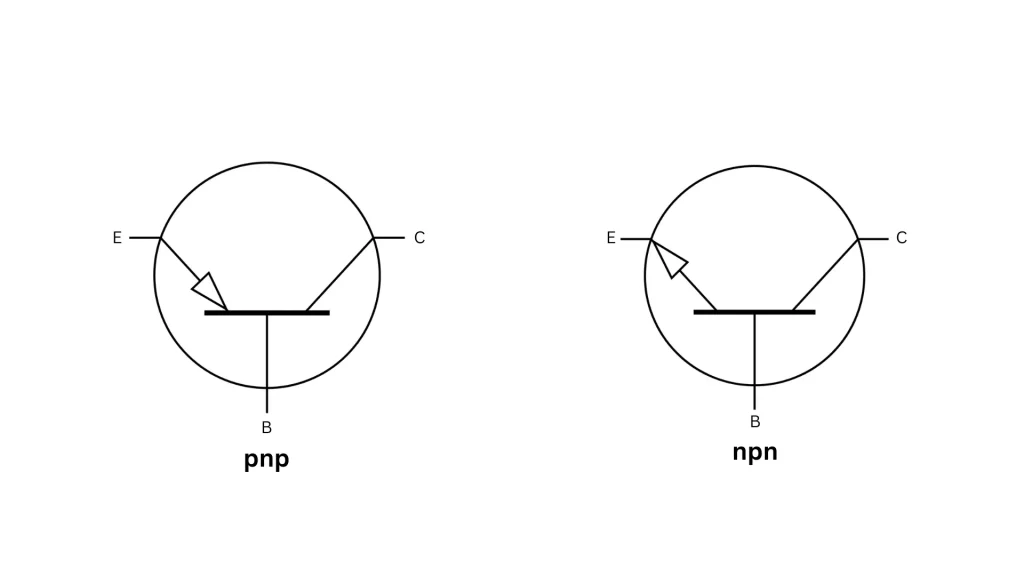
Symbol of transistor
PNP and NPN transistors have slightly different symbols. The only difference they have is the emitter terminal shown in Figure (1). In the emitter terminal, an arrow indicates the conventional current flowing direction. In the PNP transistor, the arrow points inside the transistor and in NPN the arrow points outward the transistor. Proper biasing can be applied considering the current direction indicated in the symbol of the transistor.
How do transistors work?
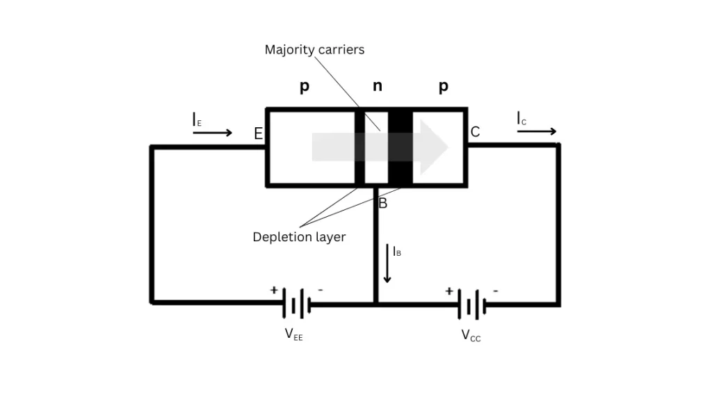
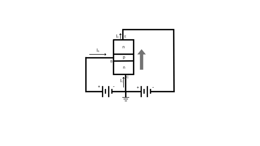
We can understand how transistors work by an example of a PNP transistor as shown in Figure (2). If we apply forward bias to one p-n junction and reverse bias to another p-n junction. Because of the forward biasing of the first p-n junction, the majority carrier (holes) of the p-type material flows to the n-type material of the junction. After that, the majority of carriers have two paths. One is the base current IB and the other is the second n-type to p-type junction.
The base of the transistor is a lightly doped and thin layer that’s why it has low conductivity. As a result, a small amount of current flows through the base terminal as IB current. A large amount of the majority carries flows to n-type to p-type material even though the second p-n junction is reverse-biased. Because the majority carriers in the p-type material are minority carriers in the n-type material, we know that in the diode if we apply reverse bias we can get a small amount of current because of minority carriers flow.
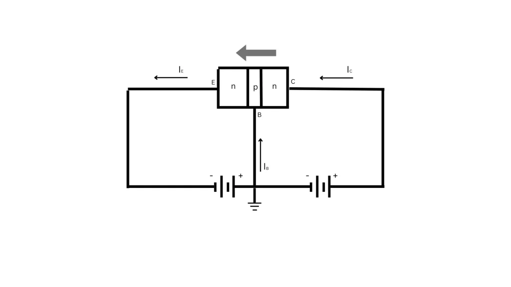
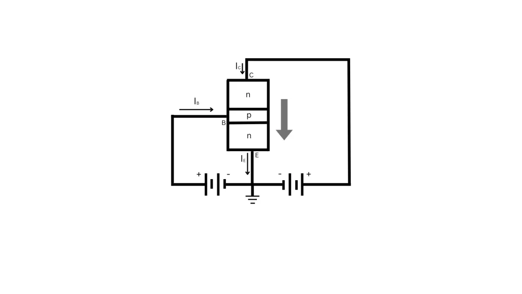
As a result, the huge amount of majority carrier flows through the depletion layer of the p-n junction. In short, we can say holes from the p-type material flow through the n-type material to the other p-type material. The operation of the NPN transistor is as same as the PNP transistor only a little difference in charge carrier. The emitter current is the sum of the base and collector current.
IE = IB + IC
Where IE is the emitter current, IC is the collector current, and IB is the base current of the transistor.
Transistor configurations
There are three main types of transistor configurations existed. They are:
- Common Base (CB) configuration
- Common Emitter (CE) configuration
- Common Collector (CC) configuration
Common Base configuration
In this configuration base of the transistor is common to both the input and the output. The emitter-base junction receives input. On the other hand, the base-collector junction gives output.
Common Emitter CE configuration
In CE configuration, an Emitter is common to both the input and the output. Base-emitter junction receives input and the collector-emitter junction gives output. CE configuration is good for the amplification process.
Common Collector CC configuration
In CC configuration collector is common to both the input and output. Base-collector junction takes input and the emitter-collector gives output.
Alpha (α) of a transistor
Alpha is the relation between IC(collector current) and IE(emitter current). The equation of alpha is given below:
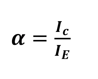
Typically, alpha ranges from 0.90 to 0.998 because IE is the addition of IC and IB. The value of IC is the closest to IE and IB is a tiny amount of current.
Beta (β) of a transistor
Beta is the relation between IC and IB. The equation of beta is given below:
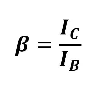
Typically, beta ranges from 50 to 400. Beta refers to how many times IC is bigger than IB current.
Uses of transistor
- The transistor is a vital element for electronics and logic circuits.
- Modern microprocessor is built using billions of billions of transistors.
- Transistor amplifies input signals. Microphones, speakers, and other electronic devices use transistors to amplify signals.
- The transistor works like a switch. So it is used to implement logical operations inside electronic circuits.
Summary
- Transistor Basics: A transistor is a semiconductor device that can function as a switch or an amplifier in electronics.
- The transistor consists of three parts: the emitter (E), base (B), and collector (C).
- There are three types of transistor configurations: common base (CB), common emitter (CE), and common collector (CC).
- Transistor performance is determined by two parameters: Alpha (α), the ratio of collector current (IC) to emitter current (IE), and Beta (β), the ratio of collector current (IC) to base current (IB).
- Transistors are crucial parts of electronics and logic circuits. They are used in the design of modern microprocessors as well as signal amplification devices. They can also be used as switches to implement logical processes in electronic circuits.