
In this tutorial, we will explain the basic principles of Inter-Integrated Circuit (I2C) communication and a closer look at the I2C hardware of the STM32 microcontroller. To get you started, we will show you how to interface the MPU-6050 accelerometer and gyroscope sensor module with the STM32 Nucleo Board using I2C.
Our other STM32 related tutorials are:
- STM32 SPI Interfacing with HAL Example Code
- STM32 ADC Interfacing with HAL code example
- How to create stm32 project in stm32cubeide with example code
- How to create a project in stm32CubeMX for Keil uvision Ide
- Stm32 Bluetooth module HC-05 interfacing with HAL code example
- Interfacing STM32 with I2C LCD : HAL example code included
What is I2C?
I2C is a serial data communication protocol used to communicate between Integrated Circuits(ICs). This protocol was created by Philips Semiconductors (now NXP) back in 1982. It is a synchronous, half-duplex, multi-master, multi-slave, packet-switched, single-ended, serial data communication protocol.
I2C signals and Modes of operation
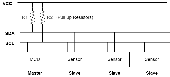
I2C is a 2-wire protocol and they are called SDA and SCL. Both SDA and SCL are bidirectional lines connected to a positive voltage supply via pull-up resistors. Both the SDA and SCL lines are held high when the bus is free.
The output stages of devices must have an open-drain or open-collector configuration. The bus capacitance limits the number of interfaces connected to the bus.
There are four different I2C modes and they are Standard-mode, Fast-mode, Fast-mode Plus, and High-speed mode. All the modes are downward-compatible means any device may be operated at a lower bus speed but Ultra Fast-mode devices are not compatible with previous versions because the bus is unidirectional.
Standard Mode (SM): Data rate up to 100 Kbits/sec,
Fast Mode (FM): Data rate up to 400 Kbits/sec
Fast mode plus (FM+): Data rate up to 1 Mbits/sec
High-Speed Mode (HS-Mode): Data rate up to 3.4 Mbits/sec
Understanding I2C protocol
In I2C, data transfer is always initiated by the master on the SDA line. Master first produces a start condition and after the start condition, the address phase follows. The address phase contains 8 bits, First 7 bits are the address of the slave, and the remaining bit decides the read or write operation.
If the Read/Write bit is 0 that indicates the master will write the data to the slave and if the bit is 1 that indicates the master will read data from the slave.
After sending the addressed slave will compare the data with its own address. If the address matches slave will send an acknowledgment bit to the master and the master receive the acknowledgment bit.
Once the master receives the Acknowledge bit, the master will start the read or write operation to the slave according to the read/write bit sent by the master earlier in the address phase. If the slave receives data it will send the Acknowledgement again or if the master receives the data then the master will send the Acknowledgement.
If the master wants to send or receive more data, it can send or receive more data. If the master wants to end communication, it will generate a stop bit to close the communication.
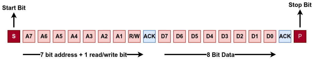
Please note that Every byte put on the SDA line must be eight bits long and each byte must be followed by an Acknowledge bit. Data is transferred with the most significant bit (MSB) first.
I2C peripheral in STM32 Microcontroller
Hardware Overview of I2C in STM32
I 2C (inter-integrated circuit) bus Interface serves as an interface between the microcontroller and the serial I2C bus. It provides multi-master capability and controls all I2C bus-specific sequencing, protocol, arbitration, and timing. It supports the standard mode (Sm, up to 100 kHz) and Fm mode (Fm, up to 400 kHz).
It may be used for a variety of purposes, including CRC generation and verification, SMBus (system management bus), and PMBus (power management bus).
Depending on specific device implementation DMA capability can be available for reduced CPU overload.
I2C main features in STM32
- Parallel-bus/I2C protocol converter
- Multimaster capability: the same interface can act as Master or Slave
- I2C Master features: Clock generation, Start and Stop generation
- I2C Slave features: Programmable I2C Address detection, Dual Addressing Capability to acknowledge 2 slave addresses, Stop bit detection
- Generation and detection of 7-bit/10-bit addressing and General Call
- Analog noise filter
- Programmable digital noise filter
Communication flow
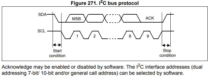
In Master mode, the I2C interface initiates a data transfer and generates the clock signal. A serial data transfer always begins with a start condition and ends with a stop condition. Both start and stop conditions are generated in master mode by the software.
In Slave mode, the interface is capable of recognizing its own addresses (7 or 10-bit), and the General Call address. The General Call address detection may be enabled or disabled by software.
Data and addresses are transferred as 8-bit bytes, MSB first. The first byte(s) following the start condition contains the address (one in 7-bit mode, two in 10-bit mode). The address is always transmitted in Master mode.
A 9th clock pulse follows the 8 clock cycles of a byte transfer, during which the receiver must send an acknowledge bit to the transmitter.
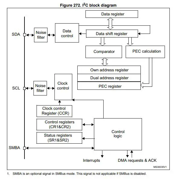
I2C Functional block diagram
You could find more information in detail in any STM32 microcontroller Reference manual. For example, If you want to know more about the STM32 I2C peripherals please click the link to download the Reference manual of the STM32F44xx microcontroller.
How to handle I2C transactions in STM32
Polling Mode
The first way is just to poll for the hardware resource until it’s ready to move on to the next step in the program instructions. However, it’s not an efficient way to handle I2C and the CPU will end up wasting so much time in a busy or waiting state.
This will happen for both transmission and reception. You have to wait until the current byte of data is transmitted so you can start the next transition and so on.
Interrupts Mode
You could use the I2C interrupts mode. In that mode, you don’t have to wait to finish the data transmission. You have a signal when I2C is done with the transmission and ready for service by CPU. This is true for both the data sent and received modes. This saves a lot of time and CPU overload. Interrupts mode is always the best way to handle events like that.
In some Critical applications like medical devices, we need everything to be as perfect and on time. The main problem with interrupts is that we can’t expect when data arrive or during which task. That can harmful to time-critical firmware.
DMA Mode
Direct memory access (DMA) is a method that allows an input or output (I/O) device to send or receive data directly to or from the main memory of the processor without the help of the CPU to speed up memory operations. To facilitate the data transfers, the I2C protocol features a DMA capability implementing a simple request/response protocol.
DMA requests are mainly generated by the Data Register of the processor. Register becoming empty in transmission and full in reception. Data transfer mainly happens between the peripheral to memory, so the CPU can perform the other tasks. This will end up saving a lot of time and is considered to be the most efficient way to handle this peripheral to memory data transfer and vice versa.
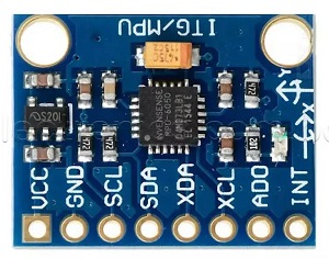
MPU6050 Accelerometer and Gyroscope Sensor
The MPU-6050 is the world’s first integrated 6-axis motion tracking device that combines a 3-axis gyroscope, 3-axis accelerometer, and a Digital Motion Processor™ (DMP) all in a small 4x4x0.9mm package. With its dedicated I2C sensor bus, it directly accepts inputs from an external 3-axis compass to provide a complete 9-axis MotionFusion™ output. The MPU-6050 Motion Tracking device, with its 6-axis integration, onboard MotionFusion™, and run-time calibration firmware, enables manufacturers to eliminate the costly and complex selection, qualification, and system-level integration of discrete devices, guaranteeing optimal motion performance for consumers.
To know more about MPU5060, you can download its datasheet from here.
Interfacing MPU6050 with STM32
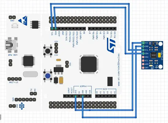
Circuit Connection
As we are using STM32 Nucleo board, I connect MPU6050 VCC to STM32 Nucleo 3.3V, Ground to Ground, SCL to SCL(PB8) and SDA to SDA (PB9)
Component List
[wptb id=933]
For troubleshooting, some extremely useful test equipment
[wptb id=890]
Affiliate Disclosure: When you click on links to make a purchase, this can result in this website earning a commission. Affiliate programs and affiliations include, but are not limited to Amazon.com
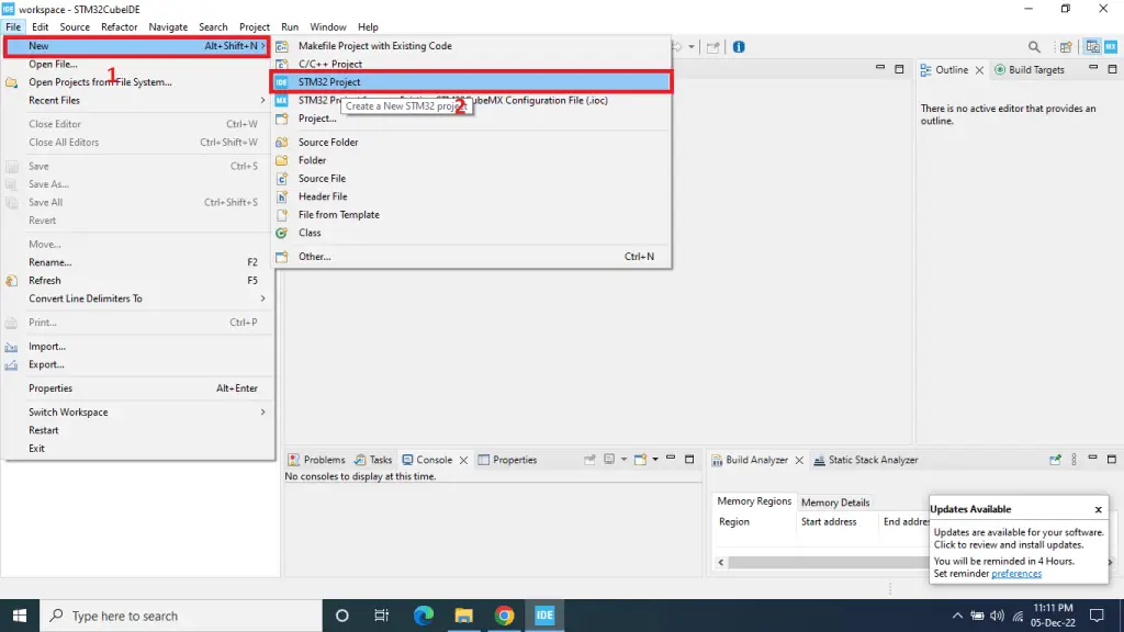
Preparing STM32CubeIDE
After the circuit connection, Our next step is to prepare the STM32Cube IDE. Open the Cube IDE and go to File > New > Stm32 project
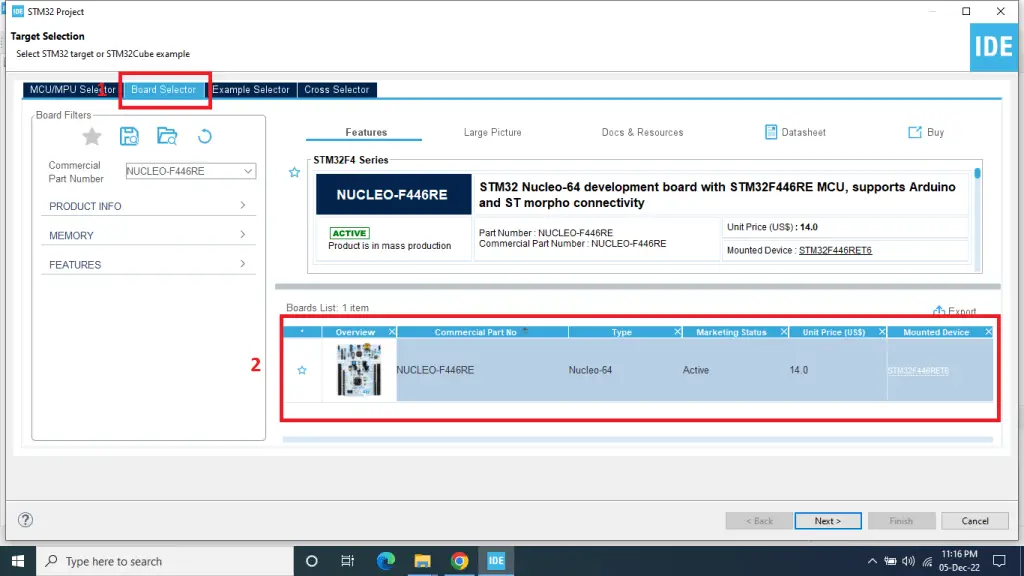
After that select the board from Board Selector tab. As I am using STM32 Nucleo board thats why I select it.
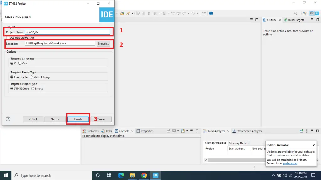
Then write the Project Name and choose the Location then click Finish.
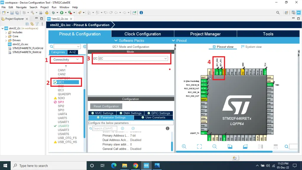
Select the Device Configuration Tool and Enable I2C1. Then select the pin PB8 as SCL and PB9 as SDA.
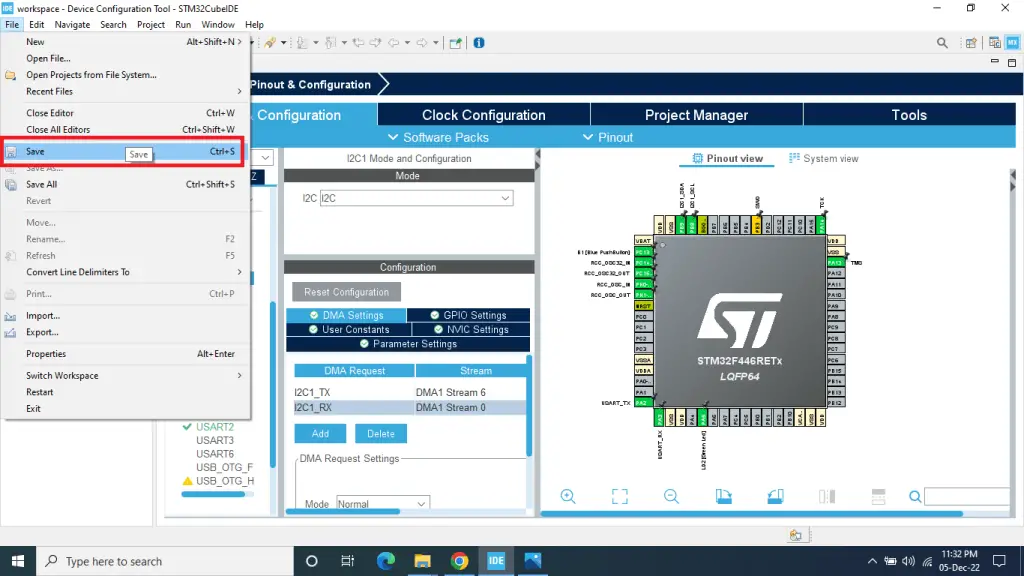
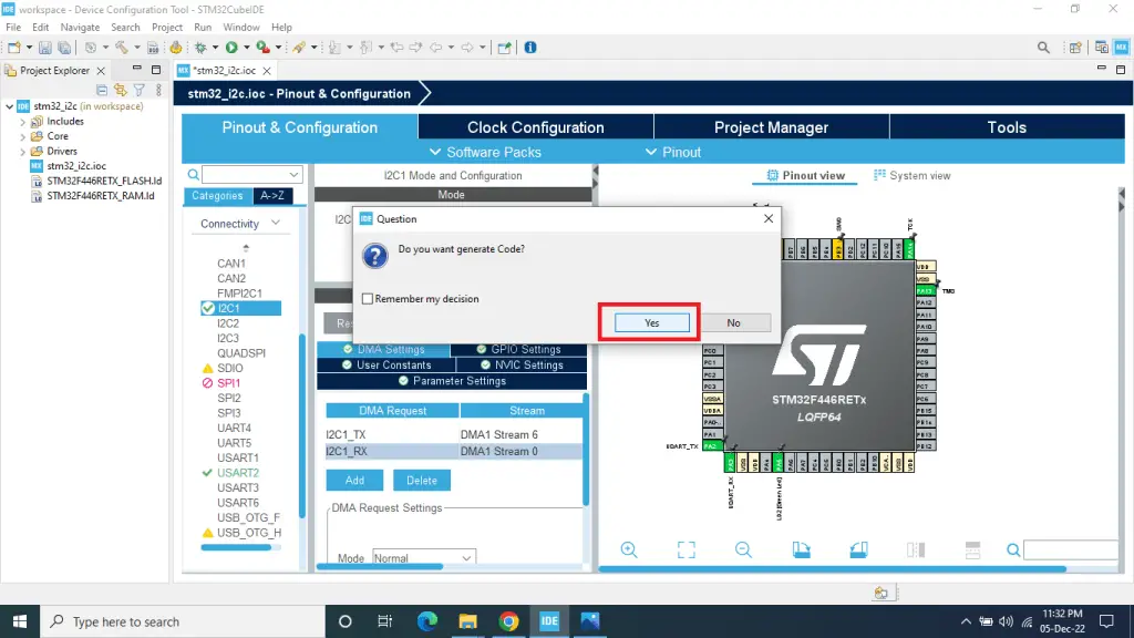
After that Save the Project and Generate the code.
STM32 I2C code for MPU6050
After Preparing the circuit and Stm32Cube IDE copy the code to your IDE. Then build and upload the code to the stm32 microcontroller.
Or, If you want to create a project in stm32CubeMX for Keil uvision IDE then we have already publish a article in this topic. Please click the link blow to visit the article
How to create a project in stm32CubeMX for Keil uvision Ide
For demonstration purposes, we are using polling mode in the program. You can use Interrupt or DMA mode. We program the sensor for Accelerometer value. You can also get the Gyroscope value by reading the register of the sensor.
For writing commands to the MPU6050 memory, we use a HAL api called HAL_I2C_Mem_Write.
HAL_I2C_Mem_Write (I2C_HandleTypeDef * hi2c, uint16_t DevAddress, uint16_t MemAddress, uint16_t MemAddSize, uint8_t * pData, uint16_t Size, uint32_t Timeout);
For reading from the memory address, we use another HAL api called HAL_I2C_Mem_Read.
HAL_I2C_Mem_Read (I2C_HandleTypeDef * hi2c, uint16_t DevAddress, uint16_t MemAddress, uint16_t MemAddSize, uint8_t * pData, uint16_t Size, uint32_t Timeout);
Here is the code:
/* Includes ------------------------------------------------------------------*/
#include "main.h"

/* Private variables ---------------------------------------------------------*/
I2C_HandleTypeDef hi2c1;
DMA_HandleTypeDef hdma_i2c1_tx;
DMA_HandleTypeDef hdma_i2c1_rx;

UART_HandleTypeDef huart2;

/* Private function prototypes -----------------------------------------------*/
void SystemClock_Config(void);
static void MX_GPIO_Init(void);
static void MX_DMA_Init(void);
static void MX_USART2_UART_Init(void);
static void MX_I2C1_Init(void);

#define MPU6050_ADDRESS 0x68 << 1 // last bit is for read/write bit

//MPU6050 Register addresses. You can download the register map from internet
#define smplrt_dv_register      0x19
#define gyro_comfig_register    0x1B
#define accel_config_register   0x1C
#define accel_x_out_h_register  0x3B
#define temp_out_h_reg          0x41
#define gyro_x_out_h_register   0x43
#define pwr_mgmt_1_register     0x6B
#define who_i_am                0x75

//this array store the raw data of X,Y and Z axis of accelerometer
uint8_t Receive_Data[6];

int16_t Accel_X_RAW_DATA = 0;
int16_t Accel_Y_RAW_DATA = 0;
int16_t Accel_Z_RAW_DATA = 0;

float Ax, Ay, Az;

void PMU6050_Init(void){
    uint8_t check_val, sendData;
    HAL_I2C_Mem_Read(&hi2c1, MPU6050_ADDRESS, who_i_am, 1, &check, 1, 1000);
    if(check_val == 104){
        sendData = 0x00;
	HAL_I2C_Mem_Write(&hi2c1, MPU6050_ADDRESS, pwr_mgmt_1_register, 1, &sendData, 1, 1000);
	sendData = 0x07;
	HAL_I2C_Mem_Write(&hi2c1, MPU6050_ADDRESS, smplrt_dv_register, 1, &sendData, 1, 1000);
	sendData = 0x00;
	HAL_I2C_Mem_Write(&hi2c1, MPU6050_ADDRESS, gyro_comfig_register, 1, &sendData, 1, 1000);
	sendData = 0x00;
        HAL_I2C_Mem_Write(&hi2c1, MPU6050_ADDRESS, accel_config_register, 1, &sendData, 1, 1000);
    }
}

int main(void)
{
  HAL_Init();
  /* Configure the system clock */
  SystemClock_Config();

  /* Initialize all configured peripherals */
  MX_GPIO_Init();
  MX_USART2_UART_Init();
  MX_I2C1_Init();
  /* USER CODE BEGIN 2 */
  PMU6050_Init();

  while (1)
  {
      /* USER CODE END WHILE */
      HAL_I2C_Mem_Read(&hi2c1, MPU6050_ADDRESS, accel_x_out_h_register, 1, Receive_Data, 6, 1000);
      Accel_X_RAW_DATA = (int16_t)(Receive_Data[0] << 8 | Receive_Data [1]);
      Accel_Y_RAW_DATA = (int16_t)(Receive_Data[2] << 8 | Receive_Data [3]);
      Accel_Z_RAW_DATA = (int16_t)(Receive_Data[4] << 8 | Receive_Data [5]);

      Ax = Accel_X_RAW_DATA/16384.0;
      Ay = Accel_Y_RAW_DATA/16384.0;
      Az = Accel_Z_RAW_DATA/16384.0;

      HAL_Delay(1000);
  }
}
Please Note: I have not included some parts of the code which are auto-generated by STM32CubeIDE.