
In this tutorial, we will explain the basic principles of Analog to Digital Converter also known as ADC and closer look at the ADC hardware of the STM32 microcontroller. To get you started, we will show you how to interface the LM35 temperature sensor with the STM32 Nucleo-F446RE development Board using ADC peripheral in STM32Cube IDE and display the temperature value to a LCD display.
You may also like reading:
Our other STM32-related tutorials are:
- Getting Started with FreeRTOS in STM32
- Interfacing STM32 with I2C LCD : HAL example code included
- How to create a project in stm32CubeMX for Keil uvision Ide
- How to create stm32 project in stm32cubeide with example code
- STM32 Timer tutorial using interrupt
- Stm32 Bluetooth module HC-05 interfacing with HAL code example
Introduction
The STM32 microcontroller is a 32-bit ARM Cortex-MX based processor that’s commonly used in embedded systems application. It’s highly powerfu, versatile, and reliable, making it a popular choice for many automation applications. The STM32 has a built-in ADC peripheral that allows it to interface with analog signals.
The ADC module in STM32 Microcontroller can convert analog signals into digital signals with varying resolutions, from 12 bits to 16 bits depending on the Microcontroller and its features. The resolution determines the number of discrete values that the ADC can generate, which affects the accuracy of the conversion.
What is an ADC?
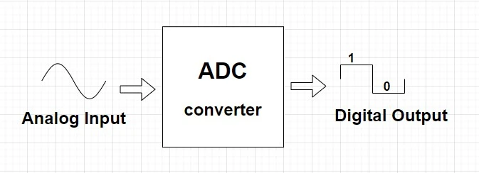
An analog to digital converter is a device or module that converts analog signals into digital signals. Analog signals are continuous signals that vary in amplitude over time, on the other hand digital signals are discrete signals that can only take on a limited number of values like 0 or 1. ADCs are used to convert signals from the analog world into digital signals that can be processed by digital circuits.
How do ADCs work?
ADCs work by sampling the input analog signal at regular intervals and quantizing the signal into a series of digital values. The process of quantization involves mapping the continuous analog signal to a finite number of digital values. The number of digital values that can be represented is determined by the number of bits in the ADC. The process of converting an analog signal to a digital signal involves three steps:
- Sampling
- Quantization
- Encoding
During the sampling process, the input analog signal is sampled at regular intervals, with the frequency of the sampling determined by the Nyquist-Shannon sampling theorem. The quantization process involves mapping the continuous analog signal to a finite number of digital values. Finally, the encoded digital values are output from the ADC for further processing.
Types of ADCs
There are several different types of ADCs. some of the most commonly used are:
Successive approximation ADCs: Successive approximation ADC is a type of analog-to-digital converter that uses a binary search algorithm to convert analog signals into digital signals. The converter first sets the most significant bit of the output to 1 and then checks whether the resulting digital value is higher or lower than the input analog signal.
Based on the result, the next most significant bit is set to 1 or 0, and the process continues until all the bits have been determined. Successive approximation ADC is widely used in applications that require high-speed and high-accuracy conversion of analog signals, such as audio and video processing, data acquisition, and control systems.
Delta-sigma ADCs: Delta-sigma ADC, also known as oversampling ADC, is a type of analog-to-digital converter that uses a technique of oversampling and noise shaping to achieve high resolution and accuracy. The converter first samples the analog signal at a very high frequency, and then uses a digital filter to reduce the noise and increase the resolution of the signal.
The filtered signal is then fed into a 1-bit digital-to-analog converter (DAC), which compares the output with the original signal and generates an error signal. The error signal is then fed back into the digital filter to improve the signal quality and reduce the quantization noise. Delta-sigma ADCs are widely used in applications that require high resolution and accuracy, such as audio and video processing, instrumentation, and measurement systems.
Flash Type ADCs: Flash Type ADC, also known as parallel ADC, is a type of analog-to-digital converter that uses a bank of comparators to convert an analog input signal into a digital output signal. The input signal is compared against a set of reference voltages, each corresponding to a particular digital output code.
The comparators generate a binary code indicating which reference voltage is closest to the input signal, and the code is converted into a digital output signal by an encoder. Flash Type ADCs are capable of high-speed conversion and are commonly used in applications such as data acquisition, radar systems, and video processing. However, they require a large number of comparators, which can be costly and consume a lot of power.
Counter type ADCs: Counter type ADC, also known as integrating ADC, is a type of analog-to-digital converter that converts an analog input signal into a digital output signal by counting the number of pulses generated by an oscillator over a fixed time interval. The input signal is integrated over the fixed time interval and the resulting voltage is compared to a reference voltage. If the integrated voltage is greater than the reference voltage, a pulse is generated and counted by a binary counter.
The process is repeated multiple times with different reference voltages until the counter reaches its maximum value, corresponding to the maximum digital output code. Counter type ADCs are simple and inexpensive but have a limited resolution and require a stable and accurate clock oscillator. They are commonly used in applications such as data acquisition, instrumentation, and control systems.
Dual slope ADCs: A dual slope ADC is a type of ADC that uses an integrator to convert an analog input signal into a digital output signal. It works by first charging up a capacitor for a fixed amount of time, while the input voltage is connected to the integrator.
Then, the capacitor is discharged for a variable amount of time, while a known reference voltage is connected to the integrator. The time it takes to discharge the capacitor is proportional to the input voltage, and this time is measured and converted to a digital value.
Please Note: Each type of ADC has its own advantages and disadvantages, and the choice of ADC will depend on the specific application.
Applications of ADCs
ADCs are used in a variety of applications, including:
- Data acquisition
- Audio recording and processing
- Video processing
- Medical imaging
- Instrumentation and control system
- Communication systems
In each of these applications, ADCs play a critical role in converting analog signals into digital signals that can be processed by digital circuits.
Factors to consider when choosing an ADC
When choosing an Analog to Digital Converter for a specific application, there are several factors that need to be considered, including:
Resolution: ADC resolution refers to the number of digital bits used to represent the analog input signal. In other words, it is the number of discrete levels or steps that the ADC can represent in the conversion process. The higher the resolution, the more accurately the ADC can represent the input signal.
For example, an 8-bit ADC can represent the input signal using 256 discrete levels, while a 16-bit ADC can represent the input signal using 65,536 discrete levels.
A higher resolution ADC can provide more accurate measurements and is often necessary for applications that require high precision. However, higher resolution ADCs also typically have slower conversion rates and higher power consumption, so the choice of ADC resolution depends on the specific requirements of the application.
Sampling rate: Sampling rate refers to the number of samples per unit of time that an analog-to-digital converter (ADC) takes of an analog input signal. It is typically measured in samples per second, or hertz (Hz). The sampling rate is important because it determines the highest frequency component of the input signal that can be accurately represented by the digital signal.
According to the Nyquist-Shannon sampling theorem, the sampling rate must be at least twice the frequency of the highest frequency component of the input signal in order to accurately reconstruct the signal.
For example, if the highest frequency component of the input signal is 10 kHz, the sampling rate must be at least 20 kHz in order to accurately capture the signal. In general, a higher sampling rate results in a more accurate representation of the input signal, but also requires more processing power and storage capacity.
Input voltage range: The input voltage range refers to the range of voltages that an electronic device or circuit can handle as an input signal without causing damage or malfunction. For example, an analog-to-digital converter (ADC) may have an input voltage range of 0 to 5 volts, which means it can accurately convert analog signals within that range to a digital signal. If the input voltage goes beyond that range, the ADC may clip the signal or become damaged.
Similarly, electronic devices such as microcontrollers, operational amplifiers, and power supplies often have specific input voltage ranges that they can safely handle. It is important to adhere to these input voltage ranges in order to ensure proper functioning and avoid damage to the device or circuit.
Noise performance: Noise performance refers to the ability of an electronic device or circuit to accurately measure or process signals in the presence of noise. Noise can be introduced by a variety of sources, such as thermal noise, electromagnetic interference, or internal circuit noise. A device or circuit with good noise performance is able to effectively filter out or minimize noise, resulting in a cleaner and more accurate output signal.
For example, a high-quality analog-to-digital converter (ADC) with good noise performance will produce digital output values that are less affected by random variations in the input signal due to noise. Similarly, a low-noise amplifier (LNA) will amplify the input signal without adding significant noise of its own.
Improving the noise performance of electronic devices and circuits is important in many applications, such as in audio and video processing, wireless communication, and medical imaging, where accurate signal processing is critical.
Power consumption: In an analog-to-digital converter (ADC), power consumption is an important consideration, as it affects the device’s performance, accuracy, and energy efficiency. The power consumption of an ADC is typically dependent on several factors, including the ADC resolution, sampling rate, input voltage range, and operating voltage.
Linearity: In electronic circuits, linearity is an important characteristic, particularly in analog circuits such as amplifiers and filters. It is also important in digital-to-analog converters (DACs) and analog-to-digital converters (ADCs), where linearity determines the accuracy of the digital output signal. Maintaining linearity requires careful design and calibration of electronic components and systems to minimize sources of non-linearity.
Please Note: The choice of ADC will depend on the specific requirements of the application.
Aanalog to Digital Converter (ADC) peripheral in STM32 Microcontroller
Hardware Overview of ADC in STM32F446RE MCU
The STM32F446RE is a popular microcontroller unit (MCU) from STMicroelectronics that includes a powerful built-in ADC. The ADC in STM32F446RE is a 12-bit successive approximation type converter that can sample up to 3.6 MSPS. It has a resolution of 4096 steps, which means it can convert analog signals into digital data with high precision.
The ADC in STM32F446RE also features a sample and hold circuit that helps to stabilize the input voltage during the conversion process. Additionally, it includes an analog multiplexer that allows the MCU to connect to multiple analog inputs. The ADC in STM32F446RE can operate in different modes, including single-conversion mode, continuous-conversion mode, and scan mode. Understanding the hardware overview of the ADC in STM32F446RE is essential for accurately reading analog signals and developing reliable applications.
To know more about the ADC peripheral please check your selected STM32 microcontroller datasheet and Reference manual. Please click the link to download the Reference manual of the STM32F44xx microcontroller for this tutorial.
How to handle ADC in STM32
Polling Mode
The STM32 microcontroller family includes a powerful Analog-to-Digital Converter (ADC) peripheral that can be configured to operate in various modes. One such mode is polling mode, where the microcontroller continuously checks the ADC status register until the conversion is complete.
In polling mode, the microcontroller can read the converted data from the ADC data register once the conversion is finished. The STM32 ADC peripheral in polling mode is suitable for applications where the sampling rate is low, and the ADC conversion time is relatively short.
Polling mode is straightforward to implement and can provide reliable results in simple applications. However, for applications with high sampling rates, interrupt-based or DMA-based ADC conversion may be more appropriate.
Interrupts Mode
In addition to polling mode, the STM32 microcontroller family also supports interrupt-based ADC conversion. In this mode, the ADC generates an interrupt request to the microcontroller once the conversion is complete, and the microcontroller can then read the converted data from the ADC data register.
Interrupt-based ADC conversion is ideal for applications where the sampling rate is high, and the microcontroller needs to perform other tasks while waiting for the conversion to complete. By using interrupts, the microcontroller can continue executing other code while waiting for the ADC conversion to finish, which can improve system performance and responsiveness.
Additionally, interrupt-based ADC conversion can help to reduce power consumption since the microcontroller can enter a low-power state while waiting for the interrupt to occur.
DMA Mode
Another mode of the STM32 ADC peripheral is Direct Memory Access (DMA) mode. In this mode, the ADC data is directly transferred to memory without any intervention from the microcontroller’s CPU. This mode is useful in applications that require high-speed and continuous data acquisition from multiple ADC channels.
DMA mode enables the microcontroller to offload the data transfer task to a dedicated DMA controller, which can transfer data at high speed while the microcontroller performs other tasks. By using DMA, the microcontroller can achieve higher data transfer rates, reduce CPU usage, and improve system efficiency.
However, configuring DMA can be more complex than configuring polling or interrupt-based ADC conversion, and it may require careful consideration of memory allocation and buffer management.
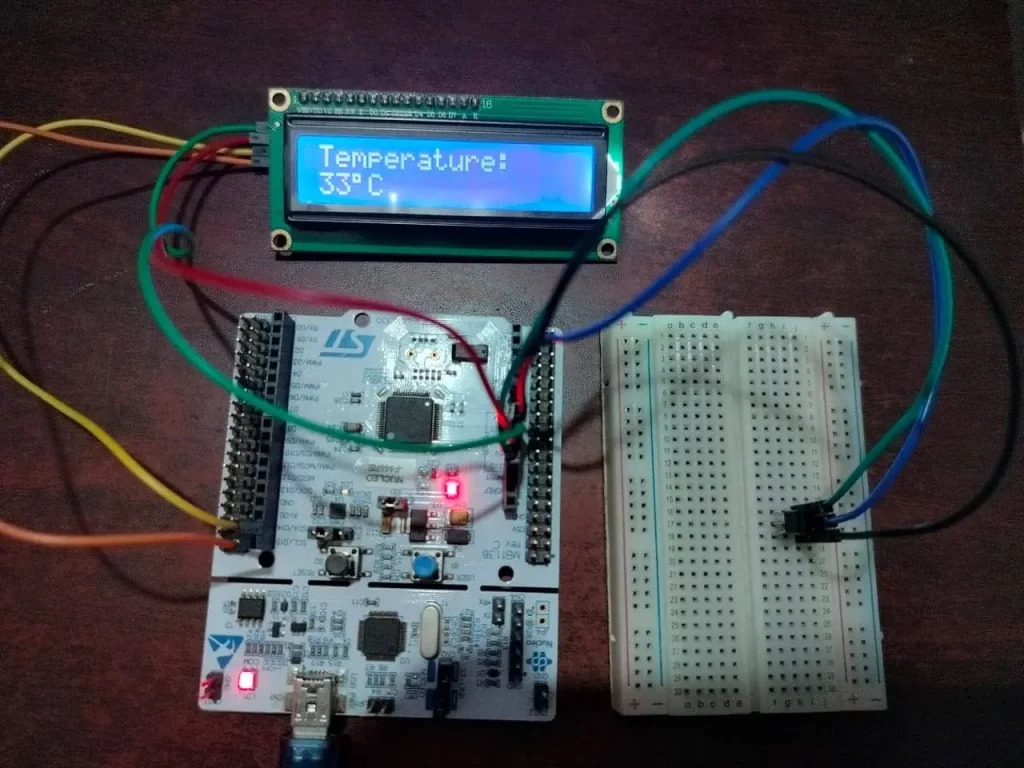
Interfacing STM32 with LM35 temperature sensor by using ADC peripheral: The project
In this section of the tutorial, we will build a real world project by interfacing STM32 Nucleo-F446RE development Board with LM35 temperature sensor using ADC peripheral in Polling Mode, in the next tutorial we will cover the Interrupt and DMA Mode. We will display the Temperature value to the LCD display. We connect the display with STM32 Microcontroller by using I2C based PCF8574 I/O expender module.
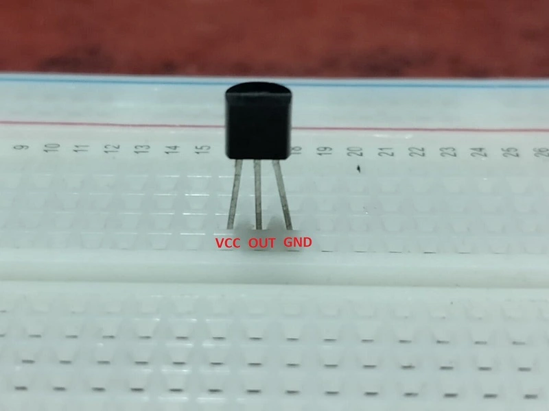
LM35 Temperature Sensor
The LM35 is a popular temperature sensor used in many electronic projects. It is a precision integrated circuit temperature sensor that provides an output voltage proportional to the Celsius temperature. The LM35 has a linear output, and its temperature sensitivity is 10 mV per degree Celsius. The sensor can measure temperatures in the range of -55°C to +150°C with an accuracy of ±0.5°C. The LM35 is easy to use and requires no external calibration or trimming. It has a low output impedance and can drive long cables without significant signal degradation. The LM35 temperature sensor is widely used in industrial, automotive, and medical applications, as well as in hobbyist projects.
Preparing I2C LCD display for STM32 Microcontroller
In this project, we will use Hitachi HD44780 controller based LCD display. To prepare the LCD display for use with an STM32 microcontroller using the PCF8574 IO expender, follow these steps:
Step 1: Obtain the necessary hardware components, including an LCD display, a PCF8574 module, and an STM32 microcontroller and Connect the PCF8574 module to the I2C pins of the STM32 microcontroller. Also connect the LCD display to the PCF8574 module using the appropriate pins
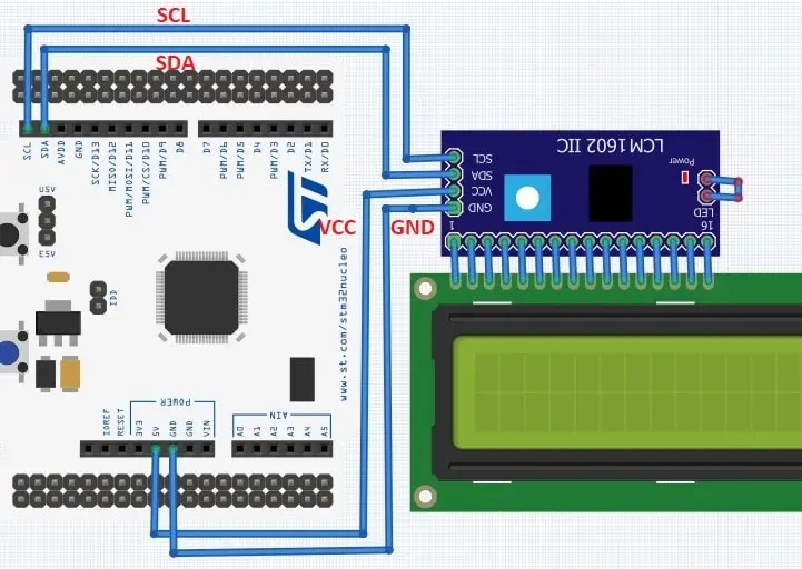
Step 2: Install the necessary software libraries for I2C communication and LCD display control on the STM32 microcontroller. To install the I2C LCD library to your project frist download the I2C LCD library from GitHub and include lcd_16x2_i2c.h and lcd_16x2_i2c.h files to the appropriate folder of the STM32Cube IDE project.
Once the I2C LCD display has been prepared, it can be used to display text and other data in various STM32-based applications. To read more about how to interface LCD I2C display with STM32 , please check the link below:
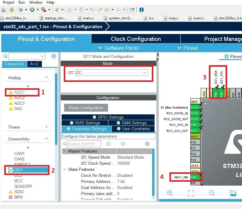
Preparing STM32Cube IDE for the project
For project creation in Stm32CubeIDE, please visit your previous tutorial. Link is given below:
After creating the project in Stm32CubeIDE, Enable the ADC1 and I2C1 peripheral from the device configuration tools of Stm32CubeIDE. For, ADC we configure GPIO A pin 0 (PA0) of the stm32 nucleo board and for I2C LCD display we configure SCL & SDA pins are GPIO B pin 8 (PB8) and GPIO B pin 9 (GPIO9) respectably.
Component List
| Component Name | Quantity | Purchase Link |
|---|---|---|
| STM32 Nucleo Development Board | 1 | Amazon |
| LM35 Sensor | 1 | Amazon |
| 16×2 I2C LCD Module | 1 | Amazon |
| Breadboard | 1 | Amazon |
| Jumper Wire Pack | 1 | Amazon |
For troubleshooting, some extremely useful test equipment
| Equipment Name | Purchase Link |
|---|---|
| Best Oscilloscope for Professionals | Amazon |
| Best Oscilloscope for Beginners and Students | Amazon |
| Logic Analyzer | Amazon |
| Best Budget Multimeter | Amazon |
| Adjustable Bench Power Supply | Amazon |
Affiliate Disclosure: When you click on links to make a purchase, this can result in this website earning a commission. Affiliate programs and affiliations include, but are not limited to Amazon.com
Circuit diagram
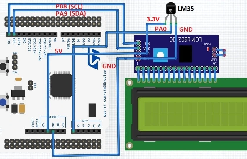
Pin connection
[wptb id=986]
Project Code and Description
/* Includes */
#include "main.h"
#include "stdio.h"
#include "string.h"
//I2C LCD Header File
#include <lcd_16x2_i2c.h>

// ADC1 Handle variable
ADC_HandleTypeDef hadc1;
// I2C1 Handle variable
I2C_HandleTypeDef hi2c1;
// UART2 Handle variable
UART_HandleTypeDef huart2;

/* Private function prototypes */
void SystemClock_Config(void);
static void MX_GPIO_Init(void);
static void MX_USART2_UART_Init(void);
static void MX_ADC1_Init(void);
static void MX_I2C1_Init(void);

/**
  * @brief  The application entry point.
  * @retval int
  */
int main(void)
{
  /* Reset of all peripherals, Initializes the Flash interface and the Systick. */
  HAL_Init();

  /* Configure the system clock */
  SystemClock_Config();

  /* Initialize all configured peripherals */
  MX_GPIO_Init(); //GPIO Initialize
  MX_USART2_UART_Init(); //USART2 Initialize
  MX_ADC1_Init(); //ADC1 Initialize
  MX_I2C1_Init(); //I2C1 Initialize
  lcd_init(); //LCD Initialize
  lcd_backlight(1); // Turn on backlight
  lcd_clear(); //Clear the LCD Screen

  // adc_value variable store the adc value,
  // temp variable store the temperature value
  int adc_value, temp;
  // store the converted voltage value
  // from analog value
  float voltage;
  // temp_str store the integer to string
  // temperature convertion
  char temp_str[20];

  /* Infinite loop */
  while (1)
  {
	  // start ADC convertion
	  HAL_ADC_Start(&hadc1);
	  // ADC poll for conversion
	  HAL_ADC_PollForConversion(&hadc1, 100);
	  // get the ADC conversion value
	  adc_value = HAL_ADC_GetValue(&hadc1);
	  // end ADC convertion
	  HAL_ADC_Stop(&hadc1);
	  // convert ADC value into voltage
	  voltage = (adc_value*3.3)/4096;
	  // convert the voltage into temperature
	  temp = voltage*100;
	  //convert the integer value to string,
	  //to display in the LCD
	  sprintf(temp_str,"%d\n", temp);
	  // LCD cursor point at row 0 column 0
	  lcd_set_cursor(0, 0);
	  // just a random string display into LCD
	  lcd_write_string("Temperature: ");
	  // LCD cursor point at row 1 column 0
	  lcd_set_cursor(1, 0);
	  // print the temperature value to LCD display
	  lcd_write_string(temp_str);
	  // LCD cursor point at row 1 column 2
	  lcd_set_cursor(1, 2);
	  // print the (degree) sign into LCD
	  lcd_send_data(0xDF);
	  // LCD cursor point at row 1 column 3
	  lcd_set_cursor(1, 3);
	  // print the (Celsius) sign into LCD
	  lcd_send_data('C');
  }
}
Please Note: We have not included some parts of the code which are auto-generated by STM32CubeIDE.